(China (Mainland))

Product Summary
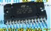
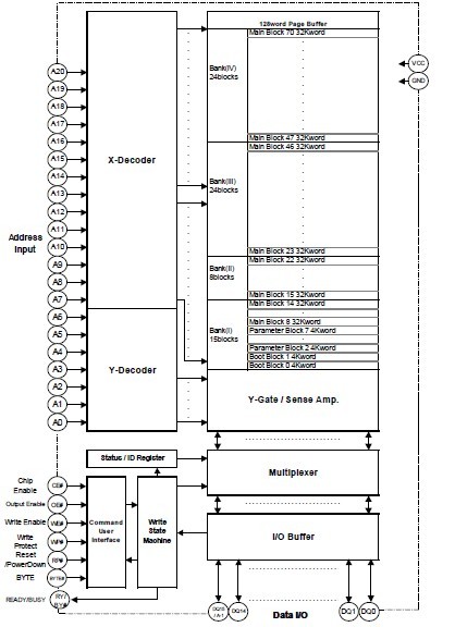
The M5M29KB331AVP is a 3.3V-only high speed 33,554,432-bit CMOS boot block FLASH Memory with alternating BGO(Back Ground Operation) feature. The BGO feature of the device allows Program or Erase operations to be performed in one bank while the device simultaneously allows Read operations to be performed on the other bank. This BGO feature is suitable for mobile and personal computing, and communication products. The M5M29KB331AVP is fabricated by CMOS technology for the peripheral circuit and DINOR IV(Divided bit-line NOR IV) architecture for the memory cell, and are available in 48pin TSOP(I) for lead free use. M5M29KB331AVP provides for Software Lock Release function. Usually, all memory blocks are locked and can not be programmed or erased, when WP# is low. Using Software Lock Release function, program or erase operation can be executed.
Parametrics
M5M29KB331AVP absolute maximum ratings: (1)VCC VCC Voltage: -0.2 to 4.6 V; (2)VI1 All Input or Output Voltage1): -0.6 to 4.6 V; (3)Ta Ambient Temperature: -40 to 85 ℃; (4)Tbs Temperature under Bias: -50 to 95 ℃; (5)Tstg Storage Temperature: -65 to 125 ℃; (6)Iout Output Short Circuit Current: 100 mA.
Features
M5M29KB331AVP features: (1)Supply Voltage: VCC = 3.0 to 3.6V; (2)Access time, Random Access: 70ns; Random Page Read: 25ns(Max.); (3)Read: 108mW; (4)Page Read: 36mW (Max.); (5)Program/Erase: 126mW(Max.); (6)Standby: 0. 33μW(typ.); (7)Deep Power Down mode: 0. 33μW(typ.); (8)Auto Program for Bank(I): Bank(IV); (9)Program Time: 30μs/word(typ.)
Diagrams
 |
 M5M28F101AFP |
Other |
|
Data Sheet |
Negotiable |
|
||||
|
M5M29F25611VP |
Other |
|
Data Sheet |
Negotiable |
|
||||
|
M5M29FB |
Other |
|
Data Sheet |
Negotiable |
|
||||
|
M5M29GB |
Other |
|
Data Sheet |
Negotiable |
|
||||
|
M5M29GB640VP |
Other |
|
Data Sheet |
Negotiable |
|
||||
|
M5M29KB |
Other |
|
Data Sheet |
Negotiable |
|
||||